The science of manipulating and capturing light with photonic crystals is particularly fundamental. Yet, it offers different applications in many essential technologies of our modern society. According to Willem Vos, his newly designed photonic crystals are of particular industrial and scientific importance. Applications are numerous because of the crystal’s flat design, tiny volume and light weight.
For example, they may improve telecommunication. Since light contains more different wavelengths than traditional electrical signals, light can carry and transfer more different channels of information at the same time. An optical wire, guiding the light, can be combined with a fast optical switch that employs photonic crystals. This crystal switch may quickly reflect or block the incoming signal of a specific light color, resulting in the signal to be passed, directed into another direction, or stopped altogether. Since this can be applied on nanoscale and with extremely high switching speeds, more information can be processed with a single device.

Increase absorption efficiency
Photonic crystals may also play a role in improving solar panels. To create an efficient solar cell, light waves should remain as long as possible inside the silicon top layer, so the silicon can optimally absorb the light and convert it into electricity. ‘If you manage to place a reflecting surface on the back of the solar cell, that preferably also redirects the light waves sideways in the silicon, the light waves travel farther inside the solar cell layer, resulting in an increased absorption efficiency,’ Vos explains. ‘Since photonic crystals are perfect mirrors for broad color ranges of light, our new flat design could very well be applied with very thin silicon solar cells. Here, they reflect the light inside the silicon in different directions, increasing light absorption and making solar panels more efficient.’
Photonic crystals
A photonic crystal is a made of a regularly-built assembly of different materials, similar to the regular pattern of carbon atoms in a diamond, yet ten thousand times bigger. Such an orderly arrangement is also present in natural photonic crystals like, for example, opal. This gem stone consists of small glass balls in a systematic arrangement, like a stack of cannon balls. Photonic crystals, like opals, reflect light in a special way, resulting in the well-known opalescent colors with their spectacular and varying color display of reds, purples, blues and greens.
The color display of photonic crystals has a fundamentally different origin than many other colored materials. Most objects get their color by absorption of certain light colors. For example, plants or fabric appear green due to the absorption of red light. However, the photonic crystals exhibit their remarkable array of colors due to reflection of different light waves (i.e. colors), that can enhance or extinguish each other: interference. When light waves enter the crystal with the right angle and color, this interference results in the distinguished spectacular color display.
Manipulate light
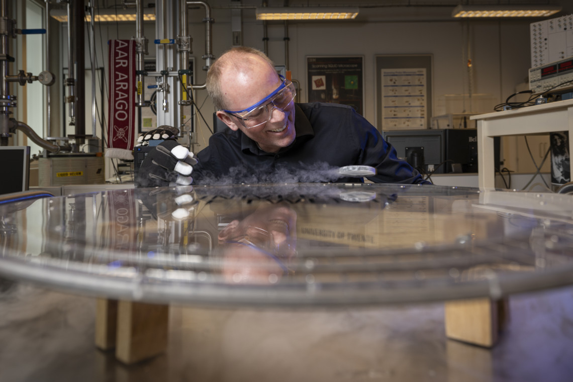
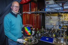
For decades, scientists used photonic crystals to increase their understanding and grip on light. They are important tools to manipulate light and harness different light colors. Inspired by the regular geometric design of gem stones, scientists have constructed new crystals by etching pores at regular distances and perpendicular to each other in wafers or blocks of silicon, the material of which integrated circuits (“chips”) in smartphones and laptops are made. In this way, a nanoscale regular 3-D pattern of hollow, air-filled pores, inside a silicon matrix can be shaped. Willem Vos and his colleagues improved the design by making the crystal flatter. ‘We found out that a very thin 3-D photonic crystal functions surprisingly well, while maintaining the essential 3-D properties,’ he says. ‘This flat design makes it much easier to integrate the crystals with other technological platforms, for instance, electronic sensors or magnetic memories.’

Impenetrable to light
The principle of catching light lies deep within the characteristics of the photonic crystal and how this influences different light colors, or light waves. When light falls on a photonic crystal, some light wavelength may enhance each other and are reflected out of the crystal: they become visible as a display of different colors. Due to this reflection, the crystal is therefore impenetrable for these light colors. Other wavelengths of light are transmitted relatively unimpeded through the crystal.
‘The size of the pores and the material used, shape the interference pattern: this determines if the color of light can enter the crystal or if it is reflected and becomes visible,’ Vos explains. ‘We can design the photonic crystal in such a way that only specific colors of light can enter, while others are reflected. We call those reflected, visible light colors ‘forbidden light’. By changing the size of the pores or replacing the silicon by a different material we can endlessly vary and create a crystal that, for example, reflects or blocks orange light only, while other light colors can enter.’

Light in prison

To manipulate light even more, the scientists went a step further and changed the special light properties of photonic crystals by modifying its regular structure. Vos: ‘Inside the crystal, we etched pores with a different diameter, perpendicular to each other. These different pores are designed in such a way that the forbidden light, for example orange, is not reflected anymore, but is now able to enter the crystal. It is like a fast lane inside the crystal, where the orange light can travel. Where the two differently-sized pores cross each other, a miniature cavity is created. The forbidden orange light, that is normally reflected, enters the crystal through the light fast lane and reaches this cavity. The light in the cavity is surrounded by the regularly-shaped photonic crystal that acts like a powerful 3-D mirror. Consequently, the orange light is reflected inside the crystal and cannot escape: it is ‘imprisoned’ inside. Measurements have confirmed this: the light energy present inside this tiny space is much higher than in the surrounding crystal.
With a better grip on manipulating and even capturing light using photonic crystals, the fundamental research of Vos and his colleagues has resulted in a concrete application, capable of improving many different technologies. Their newly designed photonic crystal has paved the way to better communication, more efficient solar panels and may benefit many more high-tech products.
willem vos
Willem Vos is Professor of Applied Physics at the University of Twente specialized in light. He collaborates with a wide array of high-tech companies like ASML, TNO, Signify, Lumileds and Demcon on researching light in the broadest sense. These joint research projects have important practical implications for product development and improvement. His recent work on photonic crystals is no exception: although very fundamental, high-tech companies see the potential application of his new photonic crystal design in a wide variety of products.